-
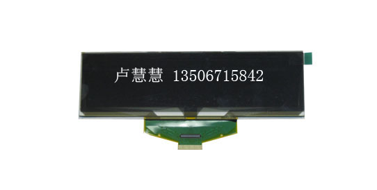
杭州清达光电技术有限公司
主营:低温显示屏,低温OLED模块 - 13506715842

杭州清达光电技术有限公司
主营:低温显示屏,低温OLED模块 18
18
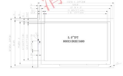
3.12寸OLED屏
1.1 Display Specifications
1) Display Mode: Passive Matrix
3) Drive Duty: 1/64 Duty
1.2 Mechanical Specifications
1) Outline Drawing: According to the annexed outline drawing
2) Number of Pixels: 256 × 64
3) Panel Size: 88.00 × 27.80 × 2.00 (mm)
4) Active Area: 76.78 × 19.18 (mm)
5) Pixel Pitch: 0.30 × 0.30 (mm)
6) Pixel Size: 0.28 × 0.28 (mm)
7) Weight: 9.95 (g)
Pin Definition
Pin Number Symbol Type Function
Power Supply
26 VCI P
Power Supply for Operation
This is a voltage supply pin. It must be connected to
external source & always be equal to or higher than VDD
& VDDIO.
25 VDD P
Power Supply for Core Logic Circuit
This is a voltage supply pin. It can be supplied
externally (within the range of 2.4~2.6V) or regulated
internally from VCI. A capacitor should be connected
between this pin & VSS under all circumstances.
24 VDDIO P
Power Supply for I/O Pin
This pin is a power supply pin of I/O buffer. It should
be connected to VDD or external source. All I/O **
should have VIH reference to VDDIO. When I/O **
pins (BS0~BS1, D0~D7, control **s…) pull high,
they should be connected to VDDIO.
2 VSS P
Ground of Logic Circuit
This is a ground pin. It also acts as a reference for the
logic pins. It must be connected to external ground.
3, 29 VCC P
Power Supply for OEL Panel
These are the most positive voltage supply pin of the
chip. They must be connected to external source.
5, 28 VLSS P
Ground of Analog Circuit
These are the analog ground pins. They should be
connected to VSS externally.
Driver
22 IREF I
Current Reference for Brightness Adjustment
This pin is segment current reference pin. A resistor
should be connected between this pin and VSS. Set the
current lower than 10uA.
4 VCOMH P
Voltage Output High Level for COM Signal
This pin is the input pin for the voltage output high level
for COM **s. A tantalum capacitor should be
connected between this pin and VSS.
27 VSL P
Voltage Output Low Level for SEG Signal
This is segment voltage reference pin.
When external VSL is not used, this pin should be left
open.
When external VSL is used, this pin should connect with
resistor and diode to ground.
Testing Pads
21 FR O
Cascade Application Connection Pin
This pin is No Connection pins. Nothing should be
connected to this pin. It should be left open individually.